A simple way to connect multiple sources of information in analogue electronic systems is by using mechanical switches, such as those illustrated in Fig. 4.2.1. In example (a) a single pole double throw switch is used to select either input A or input B to be connected to output X. Example (b) shows a rotary selector switch that can multiplex any one of eight inputs to a single output.
In digital electronics, selecting multiple data sources can be performed by combinational logic circuits. Logic signals applied to one or more data select inputs initiate the selection of data, which may be steady logic levels or whole streams of digital information. Switching digital signals in this way is much faster and more reliable than using mechanical switch contacts. Digital data selectors and multiplexers are therefore a vital part of many digital systems. The names ‘data selector’ and ‘multiplexer’ are commonly interchanged, with multiplexers called data selectors and vice versa. If there is any difference, a circuit selecting between two inputs may be called a data selector, and more complex circuits combining multiple inputs into a single output, using various methods and existing in both digital and analogue forms, would be called multiplexers.
Basic Data Select (Multiplexer) Circuits
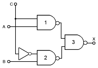
A simple data selector consisting of a single XOR gate was used in the 8 Bit Adder/Subtractor circuit shown in Figs. 4.1.5 and 4.1.6 in Module 4.1 to change the function of the circuit from addition to subtraction, but this was only required to select data B or its inverse B. The circuit shown in Fig. 4.2.2 however can select either of two completely independent data inputs.
The operation of Fig. 4.2.2 is quite straightforward and relies on ‘enabling’ either of a pair of NAND gates (1 and 2), but not both.
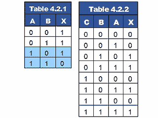
From the truth table for a NAND gate shown in Table 4.2.1 it can be seen that if one of the inputs (e.g. input A) is kept at logic 1, then the output will be the inverse of the other input. The gate is said to be enabled. If however input A is kept at logic 0, then the output will always be logic 1 whatever the state of the second input. The gate is therefore disabled, and the input cannot reach the output, even in inverted form. Gate 3 in Fig. 4.2.2 is simply combining the inputs from the other two gates. Table 4.2.2 illustrates the operation of Fig.4.2.2.
Multiplexing
The control input (C) to the circuit in Fig.4.2.2 is fed directly to gate 1, but inverted to gate 2. This ensures that whatever the logic state of C, one gate is enabled, whilst the other is disabled.
Therefore when C = 1, NAND gate 1 will be enabled and its output will be the inverse of its data input (i.e.A), and because C (in this case logic 0) is applied to the control input of gate 2 its output will be logic 1.
Applying logic 0 to input C will cause gate 1 to be disabled, making its output logic 1, and gate 2 will be enabled making its output B.
Gate 3 will therefore always have one of its inputs held at logic 1, because either gate 1 or gate 2 is disabled, whilst the other input to gate 3 will be either A or B. Gate 3 output will be the inverse of this input, so the result at the output X will be either A or B depending on the state of the control line, as can be seen from Table 4.2.2.
Note that this arrangement of three NAND gates (or four if an additional NAND gate is used in place of the inverter) works just the same as having an inverter (NOT gate) select either of two AND gates whose outputs are combined by an OR gate (De Morgan’s theorem) but uses only one Quad 2-input gate IC instead of the three required by the NOT/AND/OR solution.
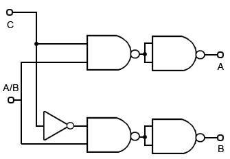
Fig. 4.2.3 A Simple De−multiplexer
De−multiplexing
Having combined, or multiplexed two data sources into one output line, it will usually be necessary at some point to separate or de-multiplex the combined data into separate outputs once more. To do this for the circuit in Fig. 4.2.2, a circuit such as that shown in Fig 4.2.3 will be required.
Two connections from the data select circuit are required to connect the data to this simple de−multiplexer, one to connect the data from output X of the data select circuit in Fig. 4.2.2 to the combined A/B input of Fig.4.2.3 and another connection from C on Fig. 4.2.2 to C on Fig. 4.2.3 to share the control signal.
Having to use two connecting lines to connect the multiplexer to the de-multiplexer to carry two signals does not apparently justify using these two extra circuits, however the principle of multiplexing demonstrated in Figs. 4.2.2 and 4.2.3 can be extended to multiplex a greater number of data inputs, and the more lines that are multiplexed in this way, the more efficient the system becomes. Also there are additional ways to use these techniques other than transferring data from one place to another, as explained in Digital Electronics Module 4.4 (Encoders and Decoders).
Multi−Bit Multiplexers
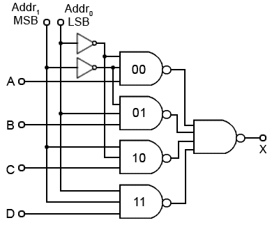
There are many uses for multiplexers. Wherever a number of signals, or logic states, need to be passed down a single communication channel such as a wire, a radio channel, or a telephone, some form of multiplexing is used. Sometimes the multiplexing and de-multiplexing can be very complex, much more so than the circuit in Figs 4.2.2 and 4.2.3. In some systems, data is transferred over very long distances, in others such as transferring data within computers, the distances may be very short. Fig. 4.2.4 shows a 4 to 1 line multiplexer, which enables a 4-bit binary number to be passed over 3 lines, one for data and two for control.
Addressing
Larger multiplexers, such as 4, 8 or 16 bit types, which are readily available in IC form, use a method of ‘addressing’ a particular data gate using a binary code. Fig 4.2.4 shows a 4 to 1 multiplexer where, in order to output data from a particular input, one of the four 3−input NAND gates must be enabled by a logic 1 on two of its inputs, leaving the third input for data. To achieve this two address lines are used, giving four possible combinations of 1 and 0.
Look carefully at the address lines. When both are at logic 0 the two inverters (NOT gates) produce logic 1s at two of the inputs to NAND gate 00. None of the other NAND gates addressed by these lines has both its address inputs at logic 1. If the least significant bit (lsb) of the address is 1 and the most significant bit (msb) is 0 then NAND gate 01 is enabled. Because two address lines can give four possible binary combinations, you should find that, counting from the top, gate 00 is enabled by the address inputs 002, gate 01 by address 012, gate 10 by 102 and gate 11 by 112.
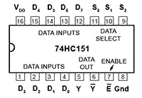
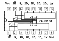
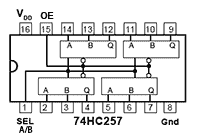
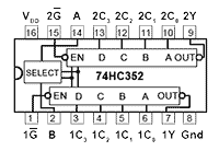
Multiplexer IC Datasheets
There are many commercially available multiplexer ICs available with a variety of extra features. The following is a list of datasheets for some basic multiplexers similar to those described in this article.
No comments:
Post a Comment