Typical applications for SR Flip-flops.
The basic building bock that makes computer memories possible, and is also used in many sequential logic circuits is the flip-flop or bi-stable circuit. Just two inter-connected logic gates make up the basic form of this circuit whose output has two stable output states. When the circuit is triggered into either one of these states by a suitable input pulse, it will ‘remember’ that state until it is changed by a further input pulse, or until power is removed. For this reason the circuit may also be called a Bi-stable Latch.
The SR flip-flop can be considered as a 1-bit memory, since it stores the input pulse even after it has passed. Flip-flops (or bi-stables) of different types can be made from logic gates and, as with other combinations of logic gates, the NAND and NOR gates are the most versatile, the NAND being most widely used. This is because, as well as being universal, i.e. it can be made to mimic any of the other standard logic functions, it is also cheaper to construct. Other, more widely used types of flip-flop are the JK, the D type and T type, which are developments of the SR flip-flop and will be studied in Modules 5.3 and 5.4.
The SR Flip-flop.
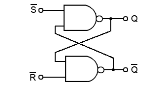
The SR (Set-Reset) flip-flop is one of the simplest sequential circuits and consists of two gates connected as shown in Fig. 5.2.1. Notice that the output of each gate is connected to one of the inputs of the other gate, giving a form of positive feedback or ‘cross-coupling’.
The circuit has two active low inputs marked S and R, ‘NOT’ being indicated by the bar above the letter, as well as two outputs, Q and Q. Table 5.2.1 shows what happens to the Q and Q outputs when a logic 0 is applied to either the S or R inputs.
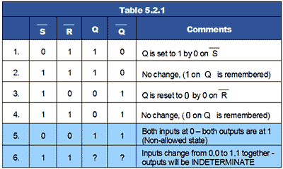
The SR Flip-flop Truth Table (Table 5.2.1)
- Q output is set to logic 1 by applying logic 0 to the S input.
- Returning the S input to logic 1 has no effect. The 0 pulse (high-low-high) has been ‘remembered’ by the Q.
- Q is reset to 0 by logic 0 applied to the R input.
- As R returns to logic 1 the 0 on Q is ‘remembered’ by Q.
Problems with the SR Flip-flop
There are however, some problems with the operation of this most basic of flip-flop circuits. For conditions 1 to 4 in Table 5.2.1, Q is the inverse of Q. However, in row 5 both inputs are 0, which makes both Q and Q = 1, and as they are no longer opposite logic states, although this state is possible, in practical circuits it is ‘not allowed’.
In row 6 both inputs are at logic 1 and the outputs are shown as ‘indeterminate’, this means that although Q and Q will be at opposite logic states it is not certain whether Q will be 1 or 0, Notice however that in the absence of any input pulses, both inputs are normally at logic 1. This is normally OK, as the outputs will be at the state remembered from the last input pulse. The indeterminate or uncertain logic state only occurs if the inputs change from 0,0 to 1,1 together. This should be avoided in normal operation, but is likely to happen when power is first applied. This could lead to uncertain results, but the flip-flop will work normally once an input pulse is applied to either input.
The SR Flip-flop is therefore, a simple 1-bit memory. If the S input is taken to logic 0 then back to logic 1, any further logic 0 pulses at S will have no effect on the output.
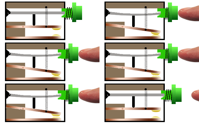
Fig. 5.2.2 Switch Bounce
Switch De-Bouncing
The fact that repeated pulses at the S (or the R) inputs are ignored after the initial pulse has set or reset the Q output, makes the SR Flip-flop useful for switch de-bouncing.
When any moving object collides with a stationary object it tends to bounce; the contacts in switches are no exception to this rule. Although the contacts may be tiny and the movement small, as the contacts close they will tend to bounce rather than close and stay closed.
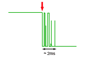
Fig. 5.2.3 Typical Switch Bounce Spikes
This causes a number of very fast on and off states for a short time, until the contacts stop bouncing in the closed position. The length of time of the bouncing may be very short, as shown in Fig. 5.2.3 where a number of fast pulses occur for about 2ms after the switch is initially closed (red arrow). For many applications this switch bounce may be ignored, but in digital circuits the repeated ones and zeros occurring after a switch is closed, will be recognised as additional switching actions.
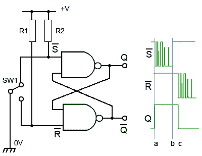
Fig. 5.2.4 SR Flip-flop Switch De-Bouncing Circuit
Switch De-Bounce Circuit
The SR flip-flop is very effective in removing the effects of switch bounce and Fig 5.2.4 illustrates how a SR flip-flop can be used to produce clean pulses using SWI, which is a ‘break before make’ changeover switch. When SW1 connects the upper contact to 0V, the S input changes from logic 1 to logic 0 and R is ‘pulled up’ to logic 1 by R1.
As soon as S is at logic 0, (at time ‘a’ in Fig. 5.2.4) output Q will be at logic 1 and any further pulses due to switch bounce will be ignored.
When SW1 is switched to the lower contact, there will be a short time (between times ‘b’ and ‘c’ in Fig. 5.2.4) when neither S or R is connected to 0V. During this time S returns to logic 1, therefore both inputs will be at logic 1 until time ‘c’, when SW1 connects R to 0V and Q is reset to logic 0 completing the output pulse. The use of a ‘break before make’ rather than a ‘make before break’ switch is important, as it ensures that during the changeover period (time ‘b’ to time ‘c’ in Fig. 5.2.4) both inputs are at logic 1 rather than the non-allowed state where both inputs would be logic 0. This ensures that outputs Q and Q are never at the same logic state.
Although, during the change over of SW1 both inputs are at logic 1, this does not produce the indeterminate state described in Table 5.2.1, as one or other of the inputs is always at logic 0 before both inputs become logic 1.
The RS Latch
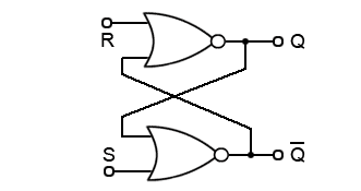
Flip-flops can also be considered as latch circuits due to them remembering or ‘latching’ a change at their inputs. A common form of RS latch is shown in Fig. 5.2.5. In this circuit the S and R inputs have now become S and R inputs, meaning that they will now be ‘active high’.
They have also changed places, the R input is now on the gate having the Q output and the S input is on the Q gate. These changes occur because the circuit is using NOR gates instead of NAND.
RS Latch Truth Table (Table 5.2.2)
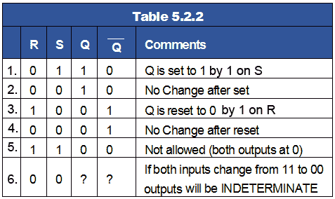
- Q is set to 1 when the S input goes to logic 1.
- This is remembered on Q after the S input returns to logic 0.
- Q is reset set to 0 when the R input goes to logic 1.
- This is remembered on Q after the R input returns to logic 0.
- If both inputs are at logic 1, Q is the same as Q (the non-allowed state).
- The state of the outputs cannot be guaranteed if the inputs change from 1,1 to 0, 0 at the same time.
Timing Diagrams
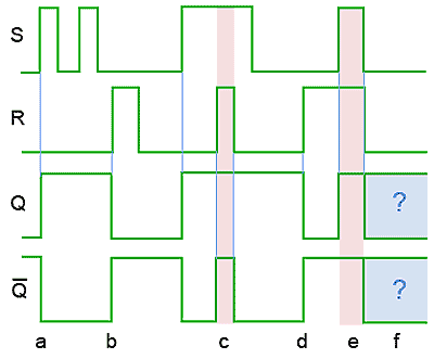
Fig. 5.2.6 RS Latch Timing Diagram
Truth tables are not always the best method for describing the action of a sequential circuit such as the SR flip-flop. Timing diagrams, which show how the logic states at various points in a circuit vary with time, are often preferred.
Fig. 5.2.6 shows a timing diagram describing the action of the basic RS Latch for logic changes at R and S. At time (a) S goes high and sets Q, which remains high until time (b) when S is low and R goes high, resetting Q. During period (c) both S and R are high causing the non-allowed state where both outputs are high. After period (c) Q remains high until time (d) when R goes high, resetting Q. Period (e) is another non-allowed period, at the end of which both inputs go low causing an indeterminate output condition in period (f).
The Clocked SR Flip-flop
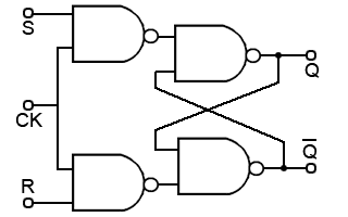
Fig. 5.2.7 shows a useful variation on the basic SR flip-flop, the clocked SR flip-flop. By adding two extra NAND gates, the timing of the output changeover after a change of logic states at S and R can be controlled by applying a logic 1 pulse to the clock (CK) input. Note that the inputs are now labelled S and R indicating that the inputs are now ‘high activated’. This is because the two extra NAND gates are disabled while the CK input is low, therefore the outputs are completely isolated from the inputs and so retain any previous logic state, but when the CK input is high (during a clock pulse) the input NAND gates act as inverters. Then for example, a logic 1 applied to S becomes a logic 0 applied to the S input of the active low SR flip-flop second stage circuit.
The main advantage of the CK input is that the output of this flip-flop can now be synchronised with many other circuits or devices that share the same clock. This arrangement could be used for a basic memory location by, for example, applying different logic states to a range of 8 flip-flops, and then applying a clock pulse to CK to cause the circuit to store a byte of data.
The basic form of the clocked SR flip-flop shown in Fig. 5.2.7 is an example of a level triggered flip-flop. This means that outputs can only change to a new state during the time that the clock pulse is at its high level (logic 1). The ability to change the input whilst CK is high can be a problem with this circuit, as any input changes occurring during the high CK period, will also change the outputs. A better method of triggering, which will only allow the outputs to change at one precise instant is provided by edge triggered devices available in D Type and JK flip-flops.
SR Flip-flop ICs
Comprising just two gates, low activated SR flip-flops are simple to implement using standard NAND gates but active low SR flip-flops (called SR flip-flops) are available as Quad packages in the LS TTL family as 74LS279 from Texas Instruments.
Circuit Symbols for Flip-flops
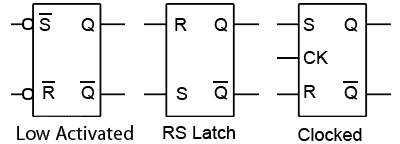
Fig. 5.2.8 SR Flip-flop Circuit Symbols
Rather than drawing the schematic circuit for individual gate versions of flip-flops it is common to draw them in block form. Some commonly used block versions of SR and RS flip-flops are shown in Fig. 5.2.8
No comments:
Post a Comment